

N
NaMLab gGmbH
Nanoelectronic Materials Laboratory for Semiconductor Research
- Employees
- 50 employees
- Founded
- Founded 2006
- Locations
- 1 location
N
NaMLab gGmbH
Nanoelectronic Materials Laboratory for Semiconductor Research
- Employees
- 50 employees
- Founded
- Founded 2006
- Locations
- 1 location
About
NaMLab gGmbH is a non-profit research organization and TU Dresden company focused on the integration and application of dielectric materials expertise to reconfigurable and energy-efficient semiconductor devices. It conducts research on novel dielectric materials, ferroelectric memory, gallium nitride power devices, and reconfigurable field-effect transistors while offering sample preparation and material characterization services to global industrial and academic partners.
Services
4Sample Preparation Services
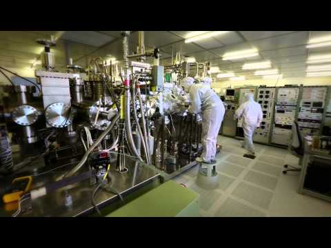
NaMLab offers semiconductor sample preparation services ranging from low-complexity 1D layer stack depositions to complex BEOL-post processing of functional devices on CMOS substrates using up to five lithography steps. Capabilities include thin film deposition via PVD, ALD, CVD, and MBE, thermal treatment up to 1200°C, e-beam and laser lithography patterning, wet chemical etching, reactive ion etching, and wafer dicing.
Electrical Characterization Services
NaMLab provides comprehensive electrical measurement and characterization services for semiconductor materials, devices, and circuits. Capabilities include C-V, C-T, C-f, and down to femto-ampere current measurements at temperatures between 5 K and 450 K and voltages up to 3000 V, direct probing on wafer level, package level reliability testing, defect spectroscopy, Hall mobility measurements, and high-frequency RF characterization.
Physical And Optical Characterization
NaMLab delivers advanced physical and optical characterization services for semiconductor materials and nanoscale structures using high-resolution scanning electron microscopy with AsB and EDX/EBSD detectors, atomic force microscopy including SSRM, C-AFM, and PFM, and multifunctional X-ray diffraction for phase analysis, layer thickness, stress state, and crystal structure determination.
Quick Info
- Followers
- …
- Employees
- 50
- Founded
- 2006
- Company type
- Tech Company
- Website
Industries1
Solution Areas4
Sub Industries2
Audience
Target Industries
Not specified yet
Customer Segments
Not specified yet
Business Model
Locations1
HeadquarterHQ
Nöthnitzer Str. 64 a, 01187 Dresden, Germany
References8
- 1.GlobalFoundries
- 2.Intel
- 3.Sony
- 4.STMicroelectronics
- 5.Infineon Technologies
Target Customer Brands
No target brands listed yet.
Recent activity
2Joined PitGrowth
NaMLab gGmbH joined the platform
Sep 2026
Company founded
NaMLab gGmbH was established
2006
Tags3
#semiconductor
#nanoelectronics
#materials